MCP 23017 GPIO
The MCP23017 integrated circuit is a micro-controller manufactured by PIC and is a digital port expander with i 2 c communication protocol (Philips 1982). Allows you to control 16 individually configurable inputs / outputs. The I / O terminals are divided into two groups of ports of 8 bits each (GPIOA and GPIOB). Let’s see the technical characteristics that this micro-controller has:
- Power supply from 1.8V to 5.5V
- Each pin can handle up to 25 mA in both output and input
- Maximum global current of 150 mA towards ground and 125 mA towards the power supply positive.
- V IL = 0.2 * Vdc (1V with 5V of Vdc )
- V IH = 0.8 * Vdc (4V with 5V of Vdc )
- V OL = 0.6V
- V OH = Vdc -0.7 (4.3V with 5V of Vdc )
- 4 kV ESD protection
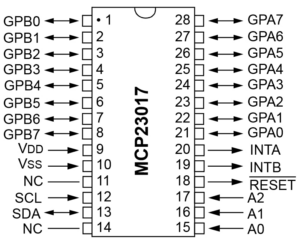 In the drawing beside we see the group A and B of the General Purpuse, Serial CLock and Serial DAta pins, two Interrupt pins and the A0-A1-A2 addressing.
The interrupts detected by two pins INTA and INTB, can be associated with the respective ports or can be logically linked so that both pins are activated if one of the ports causes an interruption.
The interrupt output can be configured to activate in two conditions (mutually exclusive):
- When an input status differs from the corresponding input port register status. It is used to indicate to the system master that an input status has changed.
- When an input state differs from a preconfigured register value (DEFVAL register). The Interrupt Capture register captures the port values at the time of the interrupt, thereby saving the condition that caused the interrupt. Power-on Reset (POR) sets registers to default values and initializes machine status.
Let’s see now how the Z80-mbc2 card uses this micro-controller.
The software of the micro-controller of the Z809-MBC2 board defines, as indicated in the following table, the peripheral management number. The values are indicated in hexadecimal base and these are the values to be used with the peripheral output instruction in the chosen programming language. The accompanying examples are written in MBASIC but are easily translate into other languages. For writing operations we have:
|
Peripheral |
Port |
Length |
|
USER LED |
0x00 |
1 byte |
|
GPIOA |
0x03 |
1 byte |
|
GPIOB |
0x04 |
1 byte |
|
IODIRA |
0x05 |
1 byte |
|
IODIRB |
0x06 |
1 byte |
|
GPPUA |
0x07 |
1 byte |
|
GPPUB |
0x08 |
1 byte |
Now let’s see what the registers of the MCP23017 indicated in the table mean.
The IODIRx register programs the pins corresponding to bits D [7..0] as input or output: 1 – input; 0 – exit. So IODIRB = 10001000 b means that the pins GPB7 and GPB3 are input, the remaining are output.
The GPIOx register contains the value of the logic status of the pins corresponding to the bits D [7..0] of the micro-controller. For example, during the writing phase, it brings the output of the GPIOA pins [7..0] to the logical state as indicated by the byte passed. On the other hand, during the reading phase, it copies the logic state of the GPIOA pins [7..0] into the peripheral input variable of the program.
The GPPUx register enables or disables the internal pull-up. If the pin is marked as input and the corresponding bit of GPPUx is at 1, then the pull-up 100 kΩ resistor is applied.
Operationally, to activate a register, a “1” must be sent to the corresponding address, then to write a “0” followed by the byte must be sent, for example:
OUT (1, register)
OUT (0, byte)
Instead to read the log:
OUT (1, register)
byte = INP (0)
Let’s now look at the RTC. From the previous table we see that RTC has as peripheral address 84 16 (132 10 ). Then we activate the RTC registers with
OUT 1, 132
Recall that RTC contains 8 registers: seconds, minutes, hours, days, months, year, temperature. These can be read sequentially via the input instruction:
INP (0)
Seconds and minutes range from 0 to 59; hours from 0 to 23; days from 0 to 31; month from 1 to 12; year from 0 to 99; temperature in degrees centigrade from -128 to 127. Let’s see the example attached to the Z80-MBC2 that allows you to read date and time from the RTC:
10 REM ***************************************
11 REM
12 REM ORARIO e DATA da RTC
13 REM
14 REM ****************************************
15 OUT 1,132 : REM Invia il comando 0x84 per leggere i registri dell’RTC
20 SECONDI = INP(0) : REM legge il numero di secondi
30 MINUTI  = INP(0) : REM legge il numero di minuti
40 ORE     = INP(0) : REM legge il numero delle ore
50 GIORNI  = INP(0) : REM legge il numero dei giorni
60 MESI    = INP(0) : REM legge il numero dei mesi
70 ANNO    = INP(0) : REM legge il numero degli anni
80 TEMP    = INP(0) : REM legge il valore della temperatura
83 IF TEMP < 128 THEN 90 : REM se la temperatura è inferiore a 128 è corretta
85 TEMP = TEMP – 256 : REM complemento a 2 per ricondurla tra -128 e 127
90 PRINT
100 PRINT "L’orario è: "
110 PRINT ORE; : PRINT ":"; : PRINT MINUTI; : PRINT ":"; : PRINT SECONDI
120 PRINT "La data è: "
125 ANNO = ANNO+ 2000
130 PRINT GIORNI; : PRINT "/"; : PRINT MESI; : PRINT "/"; : PRINT ANNO
135 PRINT "La temperatura: ";
140 PRINT TEMP; : PRINT "gradi Centigradi"
145 PRINT
From the A0640618-2 diagram of the Z80-MBC2 motherboard we see the correspondence between the pins of the GPIO registers A and B of the MCP23017 and the J7 socket.
|
GPA0 |
18 |
GPB0 |
3 |
|
GPA1 |
16 |
GPB1 |
5 |
|
GPA2 |
14 |
GPB2 |
7 |
|
GPA3 |
12 |
GPB3 |
9 |
|
GPA4 |
10 |
GPB4 |
11 |
|
GPA5 |
8 |
GPB5 |
13 |
|
GPA6 |
6 |
GPB6 |
15 |
|
GPA7 |
4 |
GPB7 |
17 |
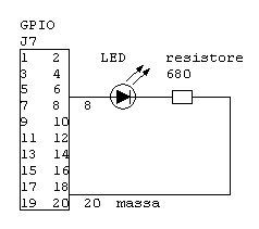
If we want a LED connected to pin 8 of J7 to be lit, we would have to act on GPA5.
As indicated in the diagram, we connect the cathode of the LED to pin 8 (GPA5) and the anode to a 680 Ω resistor which in turn is connected to ground.
We activate the IODIRA register, which in the table is 0x05 and then we impose that GPIOA.5 is an output:
OUT 1,5
OUT 0,11011111b
Now we turn on the LED by addressing the GPIOA register first and then we set the pin of GPIOA to 1.
OUT 1, 3
OUT 0, 0000000b
To turn off the LED:
OUT 1, 3
OUT 0, 00000000b
If we wanted to intercept the pressure on the USER button of the Z80-MBC2 we can operate as follows:
FLOP = 1
WHILE FLOP
      OUT 1, 128 : REM 0x80 = 128 decimale
      IF INP(0) = 1 THEN FLOP = 0
WEND
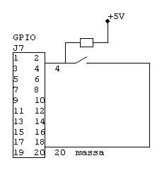
If instead the button were connected to pin 4 of J7, which corresponds to GPA7, we must also mount a pull-up resistor.
GPPUA = 7: REM 0x07
GPIOA = 3: REM 0x03
OUT 1, GPPUA
OUT 0, 100000b : REM 0x80 = 128
OUT 1, GPIOA
OUT 0, 1000000b : REM 0x80 = 128
FLOP = 1
WHILE FLOP
 OUT 1, GPIOA
 IF INP(0) = 128 THEN FLOP = 0
WEND
![]()
